Dresden, Germany / Hsinchu, Taiwan – ALLOS Semiconductors of Germany and Ennostar Corporation of Taiwan today announced a strategic partnership to bring 200 mm GaN-on-Si (gallium nitride on silicon) LED epiwafers for microLED applications into volume production. This collaboration represents a key milestone in establishing a silicon fab-compatible supply chain for microLED products.
Through this partnership, ALLOS will be able to deliver its industry-leading GaN-on-Si epiwafers at the volumes required by its customers, supporting their transition into microLED volume production. Ennostar takes on the role of ALLOS’ manufacturing partner for 200 mm GaN-on-Si LED epiwafers. With one of the world’s largest LED manufacturing infrastructures and deep expertise in high-end LED technologies, including microLEDs, Ennostar is uniquely positioned for this partnership. In addition to manufacturing, Ennostar will also contribute its advanced LED-related technologies to further enhance the product performance.
“With Ennostar we work with the best possible partner to provide our customers with a high quality and scalable supply of epiwafers. Together we can offer the industry’s best combination of highest LED efficiency and superior on-wafer and wafer-to-wafer yields for microLED chip manufacturing,” said Burkhard Slischka, co-founder and CEO of ALLOS.
“This partnership delivers competitive GaN-on-Si microLED solutions and provides a scalable production pathway compatible with standard silicon foundry processes,” said Dr. Terry Tang, President of Ennostar Corporation. “By partnering with ALLOS, we can now address the 200 mm GaN-on-Si LED epiwafer segment alongside our existing market-leading microLED solutions, offering a uniquely comprehensive value proposition to the rapidly evolving microLED industry.”
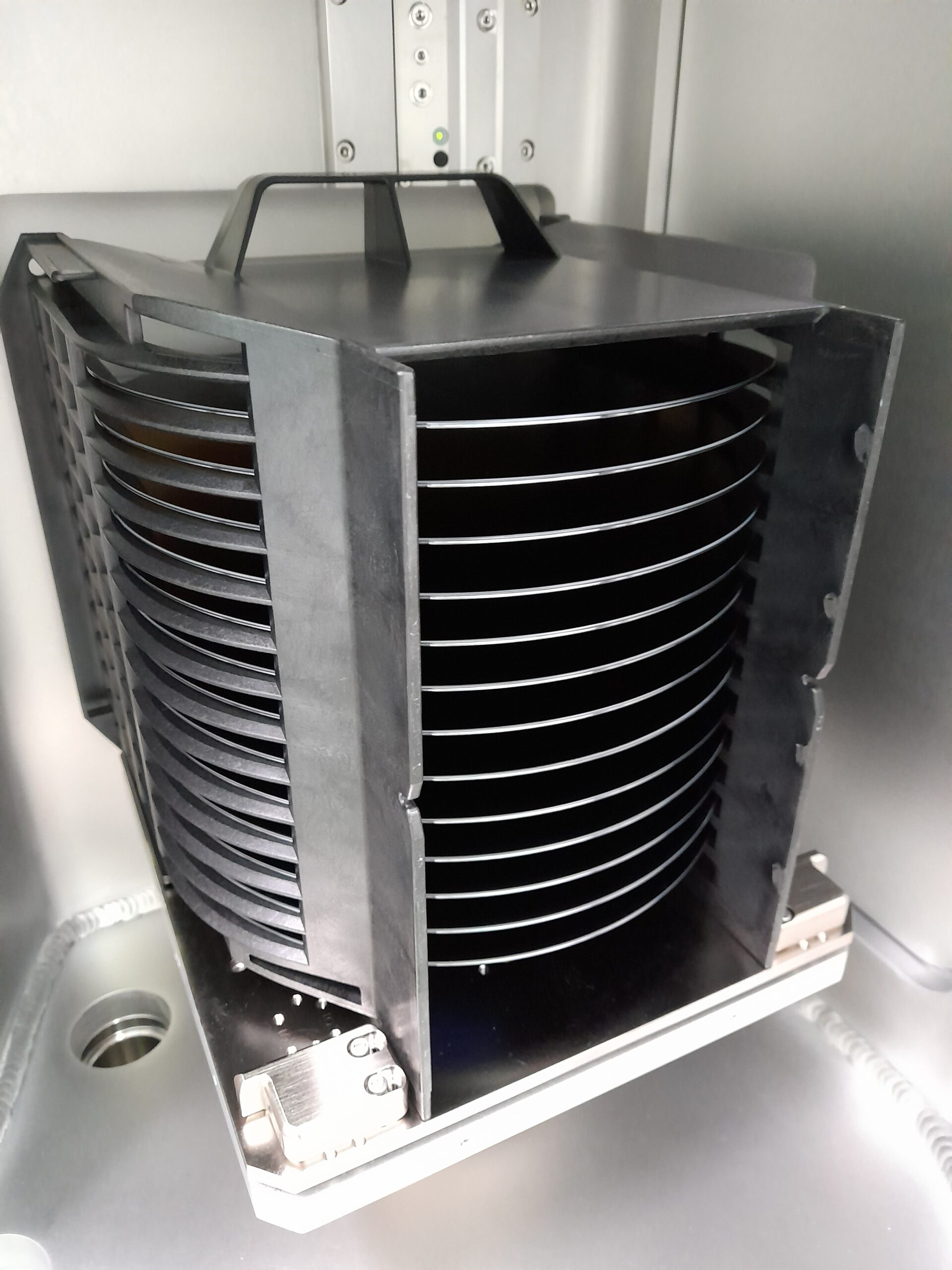
ALLOS’ epiwafer products are engineered to meet the stringent requirements of microLED applications, including uniformity, elimination of micro-defects, and optimized driving currents. Designed for compatibility with standard silicon fabs, the epiwafers are available in a thickness of 725 µm and conform to silicon industry cleanliness and contamination standards.
By combining ALLOS’ proprietary buffer and n-GaN layers with Ennostar’s cutting-edge LED layer technologies, the resulting GaN-on-Si LED epiwafers deliver brightness and energy efficiency on par with conventional GaN-on-sapphire solutions.
“We share our customers’ vision that using standard silicon fabs for microLED manufacturing will unlock the yield and cost efficiencies needed to make mass production of microLEDs economically viable,” explained Burkhard Slischka the company’s business strategy and adds, “Through our partnership with Ennostar, we can now quickly scale up epiwafer production with increasing demand for microLED products.”
The partnership also paves the way for 300 mm GaN-on-Si LED epiwafers, enabling efficient integration with 300 mm logic wafers – essential, for example, to enable ultra-fast and energy-efficient optical interconnects between AI processors and memory chips using microLED light sources. ALLOS has already demonstrated 300 mm capability since 2020 and continues to refine the technology with lead customers. For further information and product inquiries, please contact the ALLOS Semiconductors sales team.
About ALLOS Semiconductors
ALLOS Semiconductors GmbH is a GaN-on-Si epiwafer technology company focusing on microLED applications. Founded in 2014 the company has repeatedly demonstrated the industry’s best crystal quality and wafer uniformities of GaN-on-Si epiwafers specifically designed for use in standard 200 mm and 300 mm silicon wafer fabs.
The company’s proprietary technologies are protected by nearly 100 patents. ALLOS is the only company supplying both 200 mm and 300 mm GaN-on-Si LED epiwafers to customers worldwide. Its technologies are also available through licensing and technology transfer.
ALLOS’ customers are working with either foundries or in-house silicon lines to achieve breakthroughs in yield and unit cost as well as in establishing new technologies for artificial intelligence. Such breakthroughs are the critical factors to turn the customers’ microLED based solutions into volume products for the AI interface (AR displays) and AI infrastructure (optical interconnect and computing).
About Ennostar
Ennostar is a leading provider of integrated optoelectronic solutions, specializing in R&D and manufacturing III-V compound semiconductor materials. With a fully vertically integrated supply chain—from epitaxy and chip fabrication to advanced packaging and module assembly—Ennostar delivers high-efficiency, turnkey solutions to global customers.
As a pioneer in Micro LED technology, Ennostar is accelerating its commercialization. Its proprietary processes enable high uniformity, high yield, and scalable mass production, which is proposing the company at the forefront of next-generation optoelectronic innovation.
Guided by its Dual-Strategy Approach—enhancing both Field Value-Added and Solution Value-Added—Ennostar is evolving its business model to meet emerging market demands. Through its 3+1 Long-Term Development Strategy, the company focuses on four key areas: automotive, advanced displays, smart sensing, and AI optical interconnects. With Micro LED breakthroughs and system-level integration, Ennostar is shaping a brighter, smarter, and more sustainable future.
Sales and Press Contact
Alexander Loesing
Co-founder and CMO
ALLOS Semiconductors GmbH
+49-351-212-937-21
alexander.loesing@allos-semiconductors.com
Here you can download the pdf version of this press release.
Our partner Ennostar has posted a similar press release on their website in Mandarin.