ALLOS’ CEO Burkhard Slischka talks about ALLOS micro LED strategy at SSL 2017 conference in Beijing
Recently, micro LED displays have attracted tremendous attention due to reduction of energy consumption and better display quality compared with conventional TFT-LCD or OLED displays.
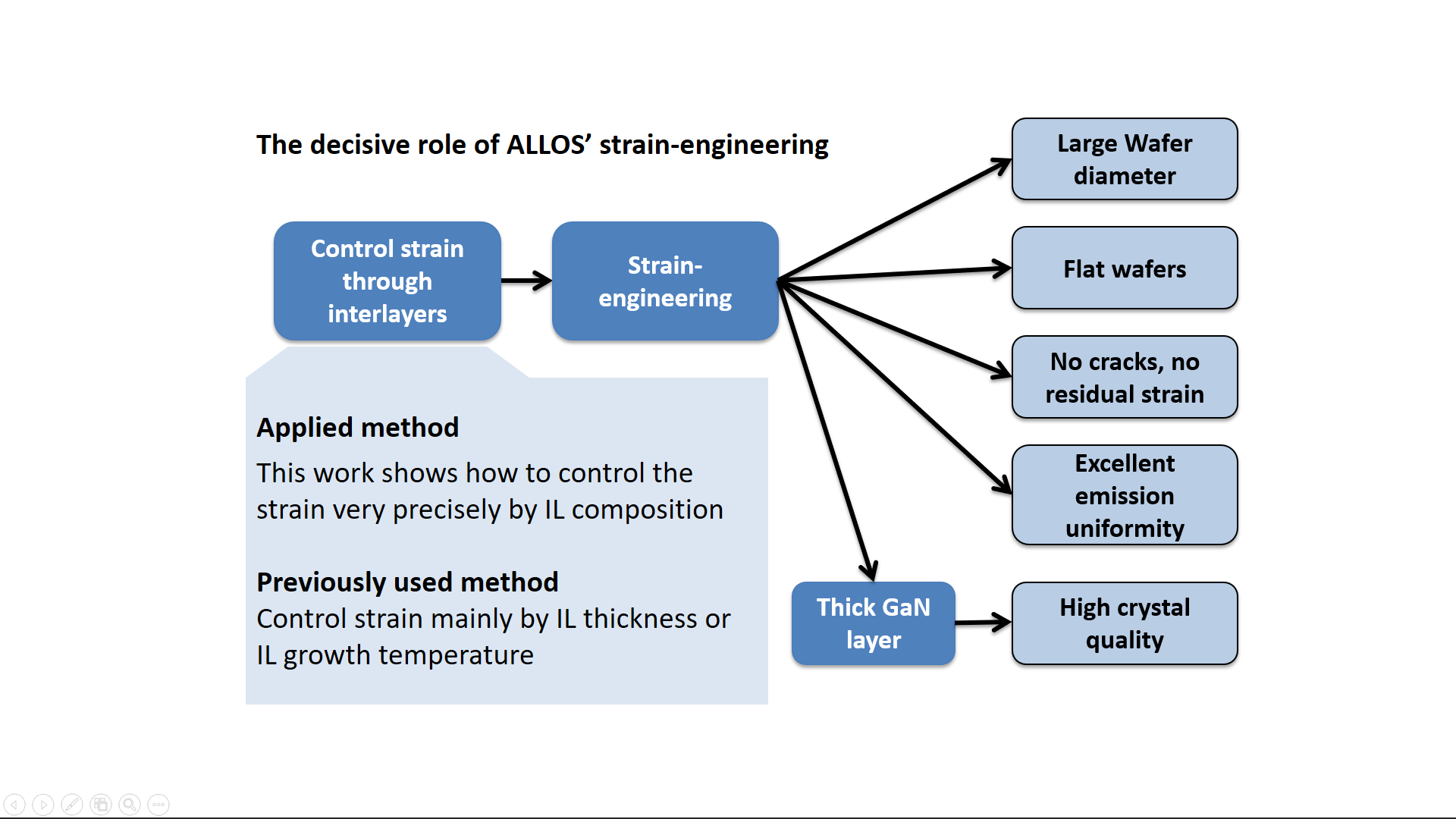
While in conventional LED making GaN-on-sapphire has the biggest market share for blue and green LED chips in micro LED GaN-on-Si has fundamental – and perhaps even enabling – advantages for manufacturability.
ALLOS can achieve large 200 mm diameter, super uniform epiwafers with small and controllable bow in a reproducible manner thanks to its unique strain-engineering technology.
In his talk at this year’s SSL conference in Beijing ALLOS’ Burkhard Slischka discussed the scientific background of ALLOS’ strain-engineering with its unique nucleation layer and interlayer technologies which enable the advantages demonstrated.
You can read and download a copy of the presentation here.
For more information please contact our sales team at: sales@allos-semiconductors.com or give us a call at: +49-351-212 937-20.